- 您现在的位置:买卖IC网 > Sheet目录697 > OP4012B (RFM)IC OPT TIMECLK 644.53125MHZ 8SMC
�� �
�
�Differential� Output� Symmetry� -� for� balanced� output� loads,� the� differential� output� symmetry� of� the� OP4012B� is� ±1%.�
�This� differential� output� symmetry� meets� the� requirements� of� the� most� demanding� high-speed� logic� families.�
�Output� DC� Voltage� Configurability� -� the� OP4012B� differential� outputs� can� be� DC-configured� to� support� a� wide� range� of� high-speed� logic� families� and� ASIC�
�drive� requirements� by� the� selection� of� four� resistors� (see� Configuring� the� OP4012B� DC� Output� Voltage� below)� and� a� logic� supply� voltage.� Each� differential�
�output� of� the� OP4012B� is� AC-coupled� to� provide� this� flexibility.�
�OP4005B� Tuning� Details�
�The� frequency� tuning� of� the� OP4012B� is� characterized� over� a� voltage� range� of� 0� to� 3.3� V.� The� tuning� voltage� applied� to� the� OP4012B� should� be� limited� to�
�this� range.� Figure� 4� shows� the� typical� locked� tuning� range� for� operation� over� -40� or� +85� °C.� The� frequency� shift� of� a� quartz� SAW� frequency� control� device�
�with� temperature� has� the� shape� of� an� inverted� parabola,� with� the� highest� frequency� occurring� around� +25� °C.� At� both� -40� and� +85� °C,� there� will� be� a� 170�
�ppm� downward� shift� in� the� frequency� of� the� SAW� device� compared� to� +25� °C.� Tuning� to� compensate� for� this� temperature� shift� is� the� same� as� tuning�
�170� ppm� higher� at� +25� °C.� This� is� well� within� the� tuning� range� of� the� OP4012B,� as� shown� in� Figure� 4.� Note� that� the� voltage� tuning� constant,� K� V� ,� is� bounded�
�between� 140� and� 300� ppm/V� under� locked� conditions� for� any� temperature� within� the� OP4012B's� specified� operating� range.�
�The� OP4012B� tuning� port� presents� a� input� impedance� greater� than� 100� kilohms� from� DC� to� 50� kHz,� and� at� least� 1� kilohm� for� any� RF� frequency� up� to� the�
�operating� frequency� of� the� OP4012B.� Most� operational� amplifiers� used� in� active� loop� filters� will� be� stable� when� driving� the� tuning� port� directly.� Special� care�
�are� should� be� taken� to� avoid� ground� loops� in� the� path� from� the� output� of� the� phase� detector� though� the� loop� filter� to� the� tuning� input� of� the� OP4012B.� For�
�most� applications,� the� bandwidth� of� the� loop� filter� in� a� OP4012B� PLL� will� be� less� than� 50� Hz,� as� discussed� in� the� example� OP4012B� PLL� application� section�
�below.�
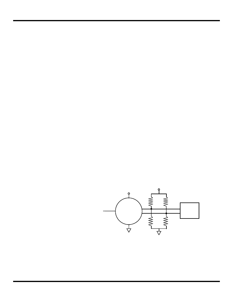
�Configuring� the� OP4012B� DC� Output� Voltage�
�Each� differential� output� of� the� OP4012B� is� AC� coupled,� allowing� the� static� DC� level� at� each� output� to� be� set� with� a� resistive� divider� to� match� the� logic� family�
�being� driven� by� the� clock.� The� parallel-equivalent� resistance� of� the� two� resistors� in� each� divider� should� be� approximately� 50� ohms.� The� supply� voltage� to�
�the� dividers,� V� LOAD� ,� should� be� two� to� three� times� the� value� of� the� static� DC� voltage,� V� DC� .�
�Referring� to� the� accompanying� figure:�
�V� DC� =� V� LOAD� *R1/(R1� +� R2)�
�and�
�50� =� R1*R2/(R1� +� R2)�
�OP4012B� DC� Output� Voltage� Adjustment�
�V� LOAD�
�3.3� Vdc�
�The� values� of� the� resistors� R2� and�
�R1� are� given� directly� as:�
�V� TUNE�
�R2�
�R2�
�V� DC�
�R2� =� 50*V� LOAD� /V� DC�
�R1� =� 1/(0.02� -� (1/R2))�
�www.RFM.com� E-mail:� info@rfm.com�
�?2008-2010� by� RF� Monolithics,� Inc.�
�OP4012B�
�R1�
�R1�
�V� DC�
�Load�
�Page� 4� of� 7�
�OP4012B� -� 2/4/10�
�发布紧急采购,3分钟左右您将得到回复。
相关PDF资料
OP4013B
IC OPT TIMECLK 693.48342MHZ 8SMC
OP4014B
IC OPT TIME CLK 627.329MHZ 8-SMC
OP4015B
IC OPT TIME CLK 780.881MHZ 8-SMC
ORD211-2030
SWITCH REED SPST-NO 10MM OKI
ORD213S-1T-1015
REED SWITCH 24VDC 1W SMD TR
ORD219-1015
SWITCH REED SPST-NO 12MM OKI
ORD2210-1020
REED SWITCH 200VDC 50W AXL
ORD2210V-2530
SWITCH REED SPST-NO 21MM OKI
相关代理商/技术参数
OP4013B
功能描述:IC OPT TIMECLK 693.48342MHZ 8SMC RoHS:是 类别:晶体和振荡器 >> 振荡器 系列:- 标准包装:1 系列:VG-4512CA 类型:VCXO 频率:153.6MHz 功能:三态(输出启用) 输出:LVPECL 电源电压:3.3V 频率稳定性:- 工作温度:-40°C ~ 85°C 电流 - 电源(最大):60mA 额定值:- 安装类型:表面贴装 尺寸/尺寸:0.276" L x 0.197" W(7.00mm x 5.00mm) 高度:0.071"(1.80mm) 封装/外壳:6-SMD,无引线(DFN,LCC) 包装:Digi-Reel® 电流 - 电源(禁用)(最大):- 其它名称:SER3790DKR
OP4014B
功能描述:IC OPT TIME CLK 627.329MHZ 8-SMC RoHS:是 类别:晶体和振荡器 >> 振荡器 系列:- 标准包装:1 系列:VG-4512CA 类型:VCXO 频率:153.6MHz 功能:三态(输出启用) 输出:LVPECL 电源电压:3.3V 频率稳定性:- 工作温度:-40°C ~ 85°C 电流 - 电源(最大):60mA 额定值:- 安装类型:表面贴装 尺寸/尺寸:0.276" L x 0.197" W(7.00mm x 5.00mm) 高度:0.071"(1.80mm) 封装/外壳:6-SMD,无引线(DFN,LCC) 包装:Digi-Reel® 电流 - 电源(禁用)(最大):- 其它名称:SER3790DKR
OP4015B
功能描述:IC OPT TIME CLK 780.881MHZ 8-SMC RoHS:是 类别:晶体和振荡器 >> 振荡器 系列:- 标准包装:1 系列:VG-4512CA 类型:VCXO 频率:153.6MHz 功能:三态(输出启用) 输出:LVPECL 电源电压:3.3V 频率稳定性:- 工作温度:-40°C ~ 85°C 电流 - 电源(最大):60mA 额定值:- 安装类型:表面贴装 尺寸/尺寸:0.276" L x 0.197" W(7.00mm x 5.00mm) 高度:0.071"(1.80mm) 封装/外壳:6-SMD,无引线(DFN,LCC) 包装:Digi-Reel® 电流 - 电源(禁用)(最大):- 其它名称:SER3790DKR
OP402-905
制造商:TT Electronics / OPTEK Technology 功能描述:
OP41
制造商:AD 制造商全称:Analog Devices 功能描述:LOW-BIAS-CURRENT, HIGH-STABILITY JFET OPERATIONAL AMPLIFIER
OP-41
制造商:AD 制造商全称:Analog Devices 功能描述:LOW-BIAS-CURRENT, HIGH-STABILITY JFET OPERATIONAL AMPLIFIER
OP413
制造商:AD 制造商全称:Analog Devices 功能描述:Low Noise, Low Drift Single-Supply Operational Amplifiers
OP413ARC/883
制造商:未知厂家 制造商全称:未知厂家 功能描述:Voltage-Feedback Operational Amplifier